 Open Access
ISSN:2151-8629(online)
Publication Frequency:Bi-monthly


Frontiers in Heat and Mass Transfer is an open access and peer-reviewed online journal that provides a central vehicle for the exchange of basic ideas in heat and mass transfer between researchers and engineers around the globe. It disseminates information of permanent interest in the area of heat and mass transfer. Theory and fundamental research in heat and mass transfer, numerical simulations and algorithms, experimental techniques, and measurements as applied to all kinds of current and emerging problems are welcome. Contributions to the journal consist of original research on heat and mass transfer in equipment, thermal systems, thermodynamic processes, nanotechnology, biotechnology, information technology, energy and power applications, as well as security and related topics.
Emerging Source Citation Index (Web of Science): 2022 Impact Factor 1.8; Ei Compendex; Scopus Citescore (Impact per Publication 2022): 2.9; SNIP (Source Normalized Impact per Paper 2022): 0.790; Google Scholar; Open J-Gate, etc.
Commencing from Volume 22, Issue 1, 2024, FHMT will transition from a bi-annual to a bi-monthly publication.
 Open Access
ARTICLE
Frontiers in Heat and Mass Transfer, Vol.22, No.1, pp. 1-14, 2024, DOI:10.32604/fhmt.2024.049335
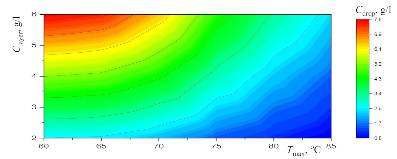
Abstract New experimental results, which are important for the potential use of small levitating droplets as biochemical microreactors, are reported. It is shown that the combination of infrared heating and reduced evaporation of saline water under the droplet cluster is sufficient to produce equilibrium saltwater droplets over a wide temperature range. The resulting universal dependence of droplet size on temperature simplifies the choice of optimal conditions for generating stable droplet clusters with droplets of the desired size. A physical analysis of the experimental results on the equilibrium size of saltwater droplets makes it possible to separate the effects related to the… More >
Graphic Abstract
Open Access
ARTICLE
Frontiers in Heat and Mass Transfer, Vol.22, No.1, pp. 15-34, 2024, DOI:10.32604/fhmt.2024.048045
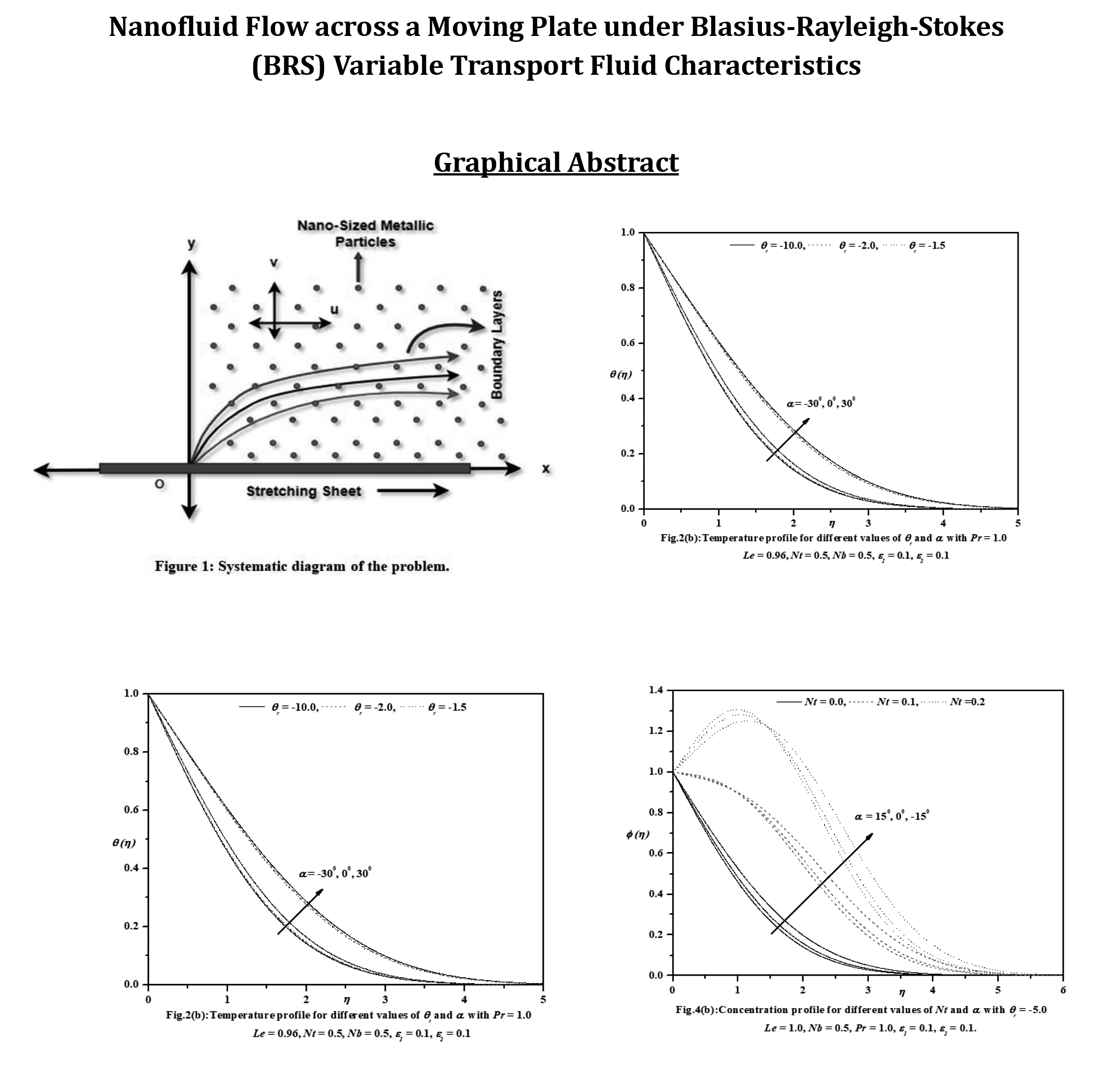
Abstract The primary aim of this research endeavor is to examine the characteristics of magnetohydrodynamic Williamson nanofluid flow past a nonlinear stretching surface that is immersed in a permeable medium. In the current analysis, the impacts of Soret and Dufour (cross-diffusion effects) have been attentively taken into consideration. Using appropriate similarity variable transformations, the governing nonlinear partial differential equations were altered into nonlinear ordinary differential equations and then solved numerically using the Runge Kutta Fehlberg-45 method along with the shooting technique. Numerical simulations were then perceived to show the consequence of various physical parameters on the plots of velocity, temperature, and… More >
Graphic Abstract
Open Access
ARTICLE
Frontiers in Heat and Mass Transfer, Vol.22, No.1, pp. 35-48, 2024, DOI:10.32604/fhmt.2024.048039
(This article belongs to this Special Issue: Passive Heat Transfer Enhancement for Single Phase and Multi-Phase Flows)
Abstract Experiments were conducted in this study to examine the thermal performance of a thermosyphon, made from Inconel alloy 625, could recover waste heat from automobile exhaust using a limited amount of fluid. The thermosyphon has an outer diameter of 27 mm, a thickness of 2.6 mm, and an overall length of 483 mm. The study involved directing exhaust gas onto the evaporator. This length includes a 180-mm evaporator, a 70-mm adiabatic section, a 223-mm condenser, and a 97-mm finned exchanger. The study examined the thermal performance of the thermosyphon under exhaust flow rates ranging from 0–10 g/sec and temperatures varying… More >
Open Access
ARTICLE
Frontiers in Heat and Mass Transfer, Vol.22, No.1, pp. 49-63, 2024, DOI:10.32604/fhmt.2024.047502
Abstract Visualization experiments were conducted to clarify the operational characteristics of a polymer pulsating heat pipe (PHP). Hydrofluoroether (HFE)-7100 was used as a working fluid, and its filling ratio was 50% of the entire PHP channel. A semi-transparent PHP was fabricated using a transparent polycarbonate sheet and a plastic 3D printer, and the movements of liquid slugs and vapor plugs of the working fluid were captured with a high-speed camera. The video images were then analyzed to obtain the flow patterns in the PHP. The heat transfer characteristics of the PHP were discussed based on the flow patterns and temperature distributions… More >
Open Access
ARTICLE
Frontiers in Heat and Mass Transfer, Vol.22, No.1, pp. 65-78, 2024, DOI:10.32604/fhmt.2024.047879
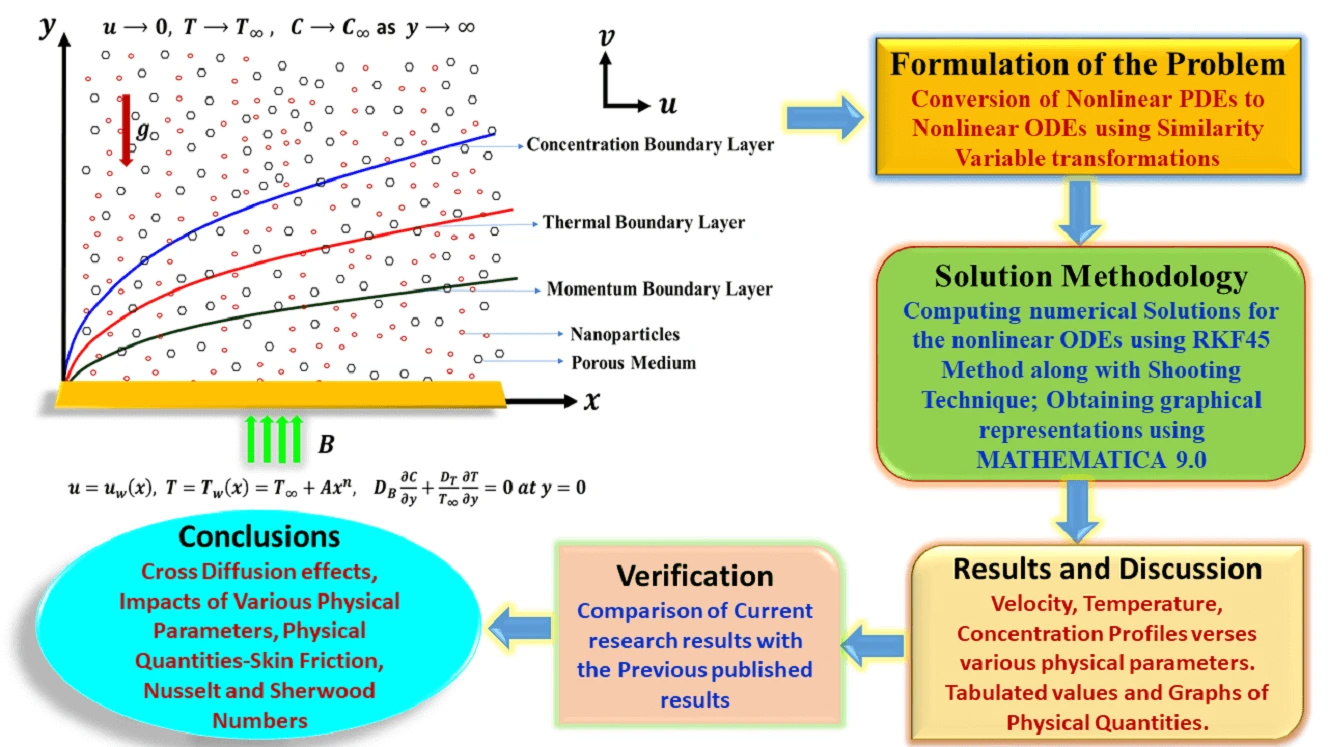
Abstract This investigation aims to analyze the effects of heat transport characteristics in the unsteady flow of nanofluids over a moving plate caused by a moving slot factor. The BRS variable is utilized for the purpose of analyzing these characteristics. The process of mathematical computation involves converting the governing partial differential equations into ordinary differential equations that have suitable similarity components. The Keller-Box technique is employed to solve the ordinary differential equations (ODEs) and derive the corresponding mathematical outcomes. Figures and tables present the relationship between growth characteristics and various parameters such as temperature, velocity, skin friction coefficient, concentration, Sherwood number,… More >
Graphic Abstract
Open Access
ARTICLE
Frontiers in Heat and Mass Transfer, Vol.22, No.1, pp. 79-105, 2024, DOI:10.32604/fhmt.2024.046891
(This article belongs to this Special Issue: Advances in Heat and Mass Transfer for Process Industry)
Abstract In the current research, a thorough examination unfolds concerning the attributes of magnetohydrodynamic (MHD) boundary layer flow and heat transfer inherent to nanoliquids derived from Sisko Al2O3-Eg and TiO2-Eg compositions. Such nanoliquids are subjected to an extending surface. Consideration is duly given to slip boundary conditions, as well as the effects stemming from variable viscosity and variable thermal conductivity. The analytical approach applied involves the application of suitable similarity transformations. These conversions serve to transform the initial set of complex nonlinear partial differential equations into a more manageable assembly of ordinary differential equations. Through the utilization of the FEM, these… More >
Graphic Abstract
Open Access
ARTICLE
Frontiers in Heat and Mass Transfer, Vol.22, No.1, pp. 107-127, 2024, DOI:10.32604/fhmt.2023.044433
Abstract Efficient and secure refueling within the vehicle refueling systems exhibits a close correlation with the issues concerning fuel backflow and gasoline evaporation. This paper investigates the transient flow behavior in fuel hose refilling and simplified tank fuel replenishment using the volume of fluid method. The numerical simulation is validated with the simplified hose refilling experiment and the evaporation simulation of Stefan tube. The effects of injection flow rate and injection directions have been discussed in the fuel hose refilling part. For both the experiment and simulation, the pressure at the end of the refueling pipe in the lower located nozzle… More >
Open Access
ARTICLE
Frontiers in Heat and Mass Transfer, Vol.22, No.1, pp. 129-139, 2024, DOI:10.32604/fhmt.2024.047825
(This article belongs to this Special Issue: Two-phase flow heat and mass transfer in advanced energy systems)
Abstract With the advancement of oilfield extraction technology, since oil-water emulsions in waxy crude oil are prone to be deposited on the pipe wall, increasing the difficulty of crude oil extraction. In this paper, the mesoscopic dissipative particle dynamics method is used to study the mechanism of the crystallization and deposition adsorbed on the wall. The results show that in the absence of water molecules, the paraffin molecules near the substrate are deposited on the metallic surface with a horizontal morphology, while the paraffin molecules close to the fluid side are arranged in a vertical column morphology. In the emulsified system,… More >
Open Access
ARTICLE
Frontiers in Heat and Mass Transfer, Vol.22, No.1, pp. 141-156, 2024, DOI:10.32604/fhmt.2024.046788
(This article belongs to this Special Issue: Computational and Numerical Advances in Heat Transfer: Models and Methods I)
Abstract This study investigates the influence of periodic heat flux and viscous dissipation on magnetohydrodynamic (MHD) flow through a vertical channel with heat generation. A theoretical approach is employed. The channel is exposed to a perpendicular magnetic field, while one side experiences a periodic heat flow, and the other side undergoes a periodic temperature variation. Numerical solutions for the governing partial differential equations are obtained using a finite difference approach, complemented by an eigenfunction expansion method for analytical solutions. Visualizations and discussions illustrate how different variables affect the flow velocity and temperature fields. This offers comprehensive insights into MHD flow behavior… More >
Open Access
ARTICLE
Frontiers in Heat and Mass Transfer, Vol.22, No.1, pp. 157-173, 2024, DOI:10.32604/fhmt.2023.045135
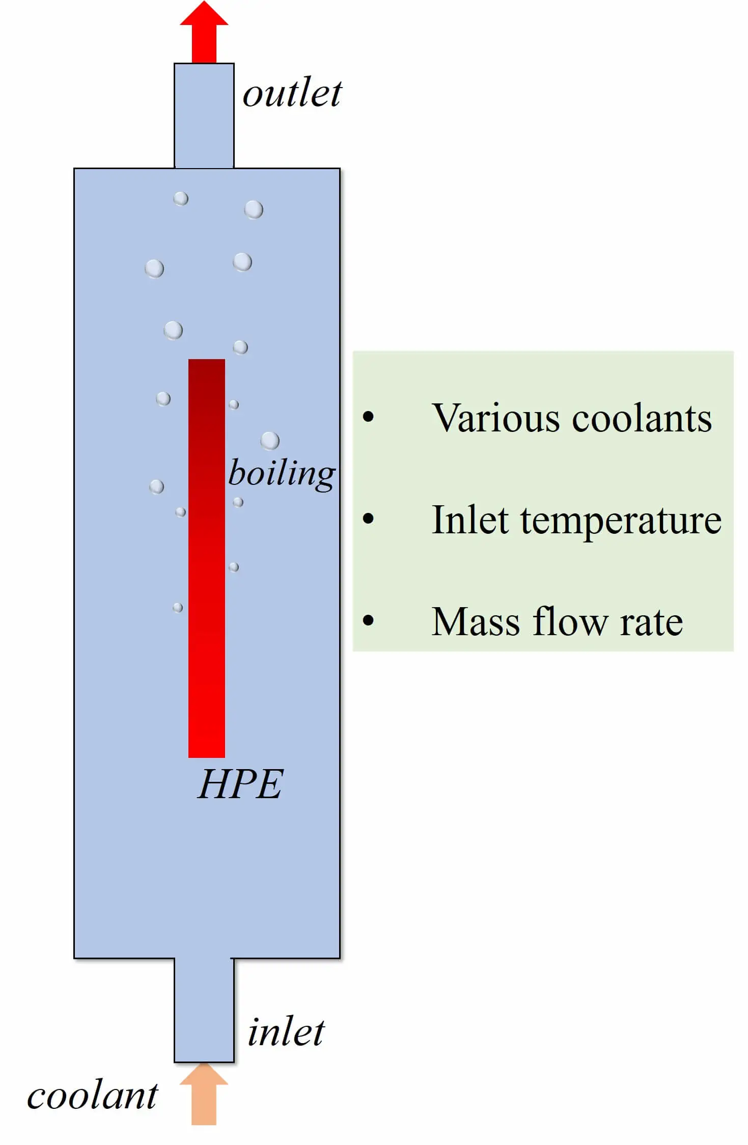
Abstract The power density of electronic components grows continuously, and the subsequent heat accumulation and temperature increase inevitably affect electronic equipment’s stability, reliability and service life. Therefore, achieving efficient cooling in limited space has become a key problem in updating electronic devices with high performance and high integration. Two-phase immersion is a novel cooling method. The computational fluid dynamics (CFD) method is used to investigate the cooling performance of two-phase immersion cooling on high-power electronics. The two-dimensional CFD model is utilized by the volume of fluid (VOF) method and Reynolds Stress Model. Lee’s model was employed to calculate the phase change… More >
Graphic Abstract
Open Access
ARTICLE
Frontiers in Heat and Mass Transfer, Vol.22, No.1, pp. 175-191, 2024, DOI:10.32604/fhmt.2023.047177
Abstract A heat exchanger’s performance depends heavily on the operating fluid’s transfer of heat capacity and thermal conductivity. Adding nanoparticles of high thermal conductivity materials is a significant way to enhance the heat transfer fluid's thermal conductivity. This research used engine oil containing alumina (Al2O3) nanoparticles and copper oxide (CuO) to test whether or not the heat exchanger’s efficiency could be improved. To establish the most effective elements for heat transfer enhancement, the heat exchangers thermal performance was tested at 0.05% and 0.1% concentrations for Al2O3 and CuO nanoparticles. The simulation results showed that the percentage increase in Nusselt number (Nu)… More >
Open Access
ARTICLE
Frontiers in Heat and Mass Transfer, Vol.22, No.1, pp. 193-216, 2024, DOI:10.32604/fhmt.2023.046832
(This article belongs to this Special Issue: Two-phase flow heat and mass transfer in advanced energy systems)
Abstract This study investigates the performance of a natural draft dry cooling tower group in crosswind conditions through numerical analysis. A comprehensive three-dimensional model is developed to analyze the steady-state and dynamic behavior of the towers. The impact of wind speed and direction on heat rejection capacity and flow patterns is examined. Results indicate that crosswinds negatively affect the overall heat transfer capacity, with higher crosswind speeds leading to decreased heat transfer. Notably, wind direction plays a significant role, particularly at 0°. Moreover, tower response time increases with higher crosswind speeds due to increased turbulence and the formation of vortices. The… More >
Open Access
ARTICLE
Frontiers in Heat and Mass Transfer, Vol.22, No.1, pp. 217-262, 2024, DOI:10.32604/fhmt.2024.047329
(This article belongs to this Special Issue: Passive Heat Transfer Enhancement for Single Phase and Multi-Phase Flows)
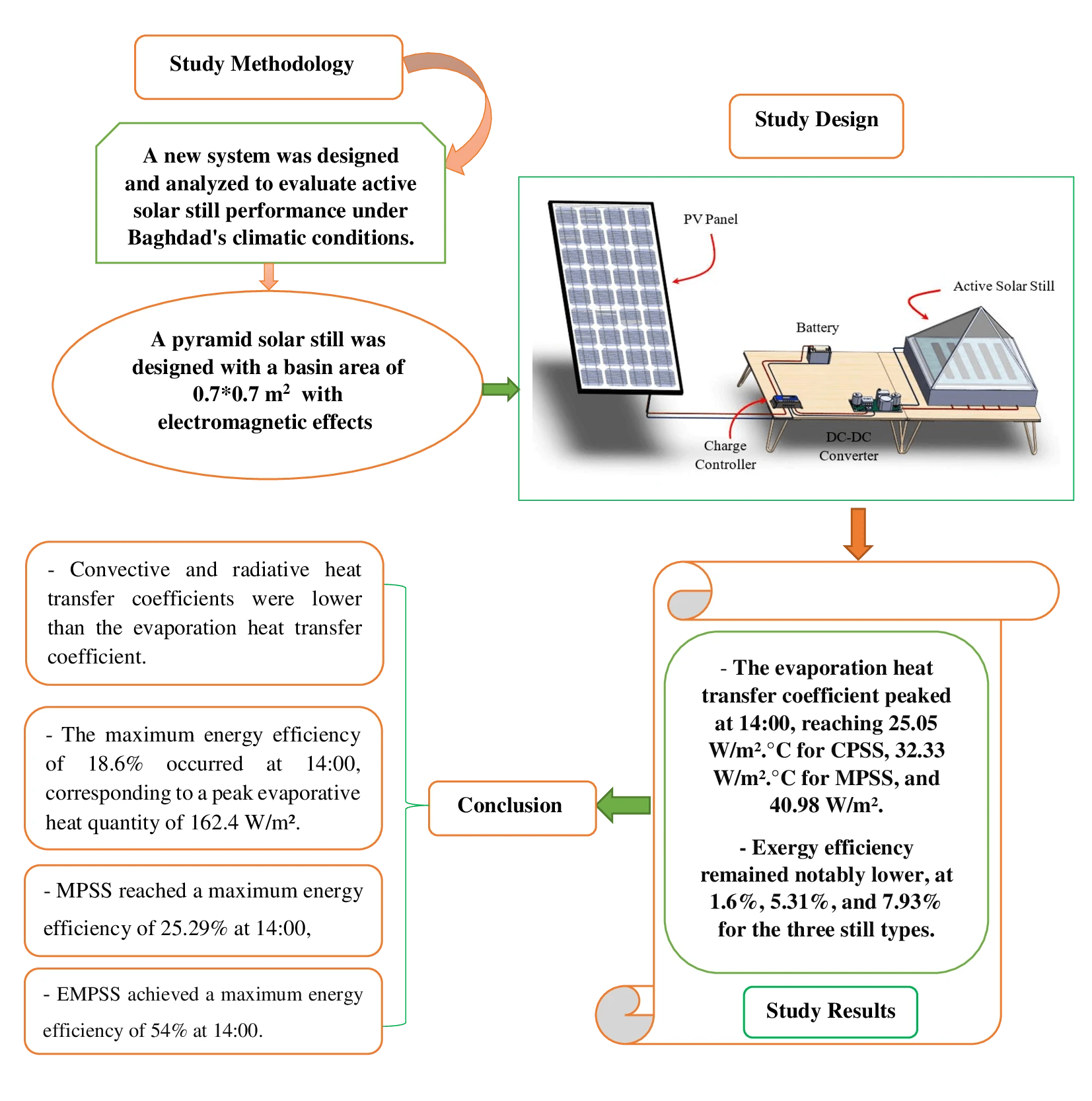
Abstract In the face of an escalating global water crisis, countries worldwide grapple with the crippling effects of scarcity, jeopardizing economic progress and hindering societal advancement. Solar energy emerges as a beacon of hope, offering a sustainable and environmentally friendly solution to desalination. Solar distillation technology, harnessing the power of the sun, transforms seawater into freshwater, expanding the availability of this precious resource. Optimizing solar still performance under specific climatic conditions and evaluating different configurations is crucial for practical implementation and widespread adoption of solar energy. In this study, we conducted theoretical investigations on three distinct solar still configurations to evaluate… More >
Graphic Abstract
Open Access
ARTICLE
Frontiers in Heat and Mass Transfer, Vol.22, No.1, pp. 263-286, 2024, DOI:10.32604/fhmt.2023.044587
(This article belongs to this Special Issue: Computational and Numerical Advances in Heat Transfer: Models and Methods I)
Abstract This paper proposes a mathematical modeling approach to examine the two-dimensional flow stagnates at over a heated stretchable sheet in a porous medium influenced by nonlinear thermal radiation, variable viscosity, and MHD. This study’s main purpose is to examine how thermal radiation and varying viscosity affect fluid flow motion. Additionally, we consider the convective boundary conditions and incorporate the gyrotactic microorganisms equation, which describes microorganism behavior in response to fluid flow. The partial differential equations (PDEs) that represent the conservation equations for mass, momentum, energy, and microorganisms are then converted into a system of coupled ordinary differential equations (ODEs) through… More >
Open Access
ARTICLE
Frontiers in Heat and Mass Transfer, Vol.22, No.1, pp. 287-304, 2024, DOI:10.32604/fhmt.2023.045038
(This article belongs to this Special Issue: Advances in Heat and Mass Transfer for Process Industry)
Abstract As compact and efficient heat exchange equipment, helically coiled tube-in-tube heat exchangers (HCTT heat exchangers) are widely used in many industrial processes. However, the thermal-hydraulic research of liquefied natural gas (LNG) as the working fluid in HCTT heat exchangers is rarely reported. In this paper, the characteristics of HCTT heat exchangers, in which LNG flows in the inner tube and ethylene glycol-water solution flows in the outer tube, are studied by numerical simulations. The influences of heat transfer characteristics and pressure drops of the HCTT heat transfers are studied by changing the initial flow velocity, the helical middle diameter, and… More >
Open Access
ARTICLE
Frontiers in Heat and Mass Transfer, Vol.22, No.1, pp. 305-315, 2024, DOI:10.32604/fhmt.2023.041882
Abstract The natural convection from a vertical hot plate with radiation and constant flux is studied numerically to know the velocity and temperature distribution characteristics over a vertical hot plate. The governing equations of the natural convection in two-dimension are solved with the implicit finite difference method, whereas the discretized equations are solved with the iterative relaxation method. The results show that the velocity and the temperature increase along the vertical wall. The influence of the radiation parameter in the boundary layer is significant in increasing the velocity and temperature profiles. The velocity profiles increase with the increase of the radiation… More >
Open Access
ARTICLE
Frontiers in Heat and Mass Transfer, Vol.22, No.1, pp. 317-339, 2024, DOI:10.32604/fhmt.2023.044706
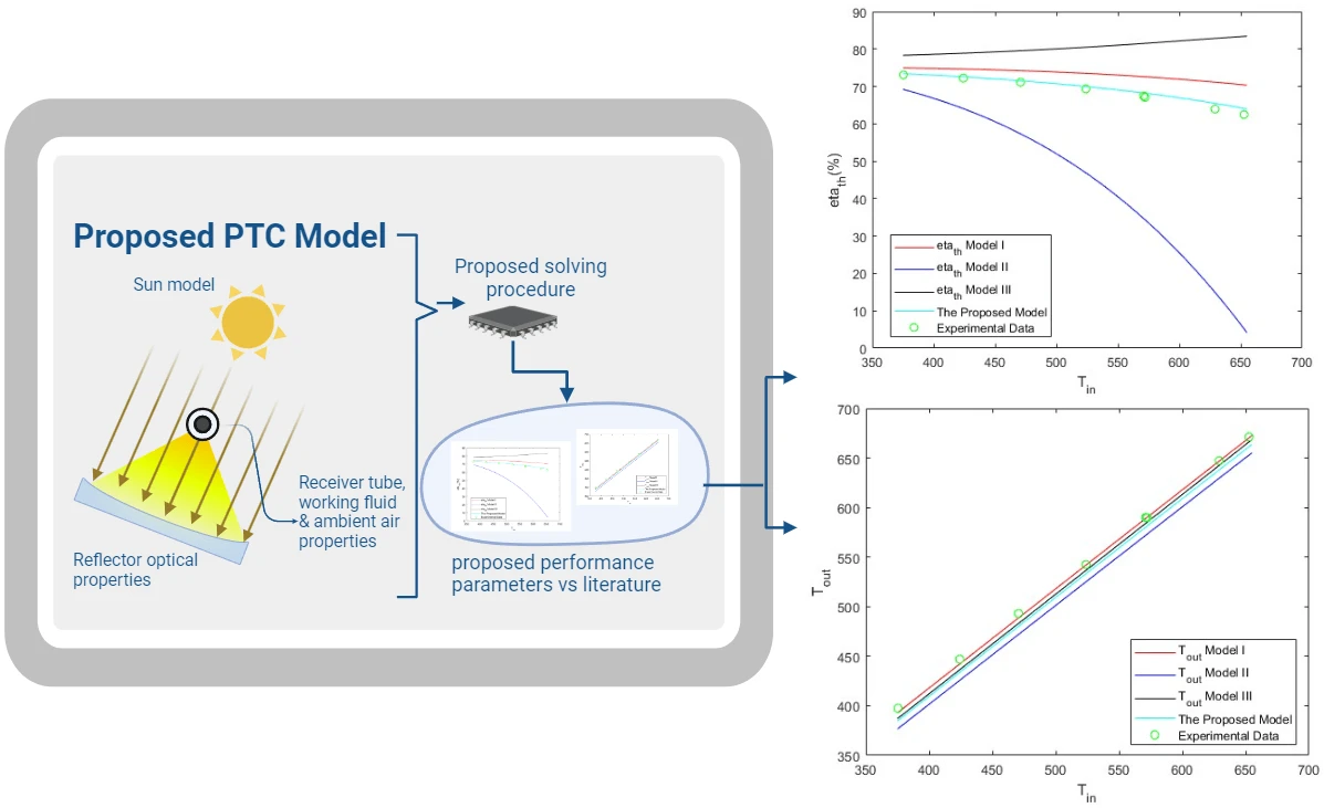
Abstract Parabolic trough solar collectors (PTCs) are among the most cost-efficient solar thermal technologies. They have several applications, such as feed heaters, boilers, steam generators, and electricity generators. A PTC is a concentrated solar power system that uses parabolic reflectors to focus sunlight onto a tube filled with heat-transfer fluid. PTCs performance can be investigated using optical and thermal mathematical models. These models calculate the amount of energy entering the receiver, the amount of usable collected energy, and the amount of heat loss due to convection and radiation. There are several methods and configurations that have been developed so far; however,… More >
Graphic Abstract
Open Access
ARTICLE
Frontiers in Heat and Mass Transfer, Vol.22, No.1, pp. 341-358, 2024, DOI:10.32604/fhmt.2024.047016
(This article belongs to this Special Issue: Heat and Mass Transfer in Thermal Energy Storage)
Abstract Faced with the world’s environmental and energy-related challenges, researchers are turning to innovative, sustainable and intelligent solutions to produce, store, and distribute energy. This work explores the trend of using a smart sensor to monitor the stability and efficiency of a salt-gradient solar pond. Several studies have been conducted to improve the thermal efficiency of salt-gradient solar ponds by introducing other materials. This study investigates the thermal and salinity behaviors of a pilot of smart salt-gradient solar ponds with (SGSP) and without (SGSPP) paraffin wax (PW) as a phase-change material (PCM). Temperature and salinity were measured experimentally using a smart… More >
Open Access
ARTICLE
Frontiers in Heat and Mass Transfer, Vol.22, No.1, pp. 359-375, 2024, DOI:10.32604/fhmt.2024.047632
(This article belongs to this Special Issue: Computational and Numerical Advances in Heat Transfer: Models and Methods I)
Abstract In this paper, experimental and numerical studies of heat transfer in a test local of side heated from below are presented and compared. All the walls, the rest of the floor and the ceiling are made from plywood and polystyrene in sandwich form ( plywood- polystyrene- plywood) just on one of the vertical walls contained a glazed door (). This local is heated during two heating cycles by a square plate of iron the width , which represents the heat source, its temperature is controlled. The plate is heated for two cycles by an adjustable set-point heat source placed just… More >
Open Access
ARTICLE
Frontiers in Heat and Mass Transfer, Vol.22, No.1, pp. 377-395, 2024, DOI:10.32604/fhmt.2023.044428
(This article belongs to this Special Issue: Computational and Numerical Advances in Heat Transfer: Models and Methods I)
Abstract A review of the literature revealed that nanofluids are more effective in transferring heat than conventional fluids. Since there are significant gaps in the illumination of existing methods for enhancing heat transmission in nanomaterials, a thorough investigation of the previously outlined models is essential. The goal of the ongoing study is to determine whether the microscopic gold particles that are involved in mass and heat transmission drift in freely. The current study examines heat and mass transfer on 3D MHD Darcy–Forchheimer flow of Casson nanofluid-induced bio-convection past a stretched sheet. The inclusion of the nanoparticles is a result of their… More >

 Submit a Paper
 Propose a Special lssue